2026.04.30
Researchers establish a reliable framework for understanding energy level alignment in perovskite solar cell interfaces using hole-collecting monolayers
Hole-collecting monolayers (HCMs) have pushed perovskite solar cells to record efficiencies, yet the fundamental mechanisms of electronic behavior and how they work at the molecular scale remain elusive. In a recent study, researchers from Japan developed the first universal model for energy level alignment at electrode/HCM/perovskite interfaces. Using fundamental energy parameters, their model successfully predicts which HCM configurations can achieve efficient charge collection, enabling the rational design of next-generation solar cells with improved performance.
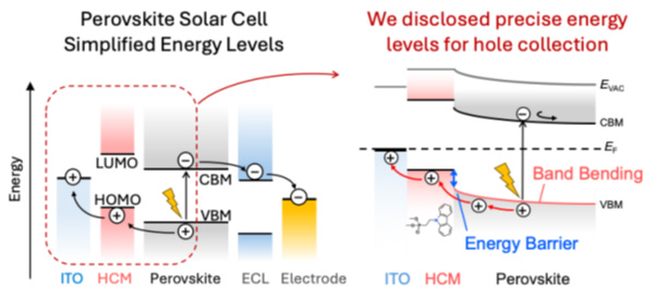
Image title: Band bending and interfacial energy barrier height as influencing factors for efficient solar cell development
Image caption: The newly developed model revealed that both the band bending phenomenon and the energy barrier height at the interface between the perovskite and the hole-collecting monolayer are critical factors in hole collection efficiency, which in turn determines the efficiency of the solar cell.
Image credit: Professor Hiroyuki Yoshida from Chiba University, Japan
Image license: Original content
Usage restrictions: Cannot be reused without permission.
Perovskite solar cells (PSCs) have emerged as one of the most promising renewable energy technologies of the past decade. Besides their remarkable power conversion rates, perovskites are lightweight in nature and can be manufactured through low-cost solution processing methods. Thus, they offer greater versatility for applications that go beyond rooftop solar cell installations, such as integration into building windows, vehicle surfaces, and portable electronics. A recent key breakthrough in PSCs has been the development of hole-collecting monolayers (HCMs)--ultra-thin layers that collect positive electrical charges ('holes') from the perovskite material. HCMs have pushed single-junction PSCs to 26.9% power conversion efficiency while improving device stability.
Despite these advances, scientists do not fully understand the fundamental mechanisms governing their molecular and electronic behavior. The way energy levels align at the interface between the electrode, the HCM, and the perovskite layer plays a central role in determining how efficiently charges move through the device. However, several competing theories, such as vacuum level alignment, Fermi level alignment, and the electrode-modified Schottky model, have been used interchangeably to model energy levels at the interface, often without clear justification. As a result, scientists today struggle to predict which HCM materials would perform well or design new ones without relying heavily on trial and error.
Fortunately, a research team led by Professor Hiroyuki Yoshida from the Graduate School of Engineering, Chiba University, Japan, has addressed this knowledge gap by developing the first universal model for energy level alignment at electrode/HCM/perovskite interfaces. Their findings, published in the Journal of Materials Chemistry A on March 14, 2026, establish a physically consistent framework that explains and provides guidelines for HCM performance across diverse material combinations. The study was co-authored by Mr. Aruto Akatsuka from Chiba University, Dr. Minh Anh Truong and Professor Atsushi Wakamiya from Kyoto University, Dr. Gaurav Kapil and Professor Shuzi Hayase from The University of Electro-Communications, Japan.
To build this model, the researchers used advanced techniques, including ultraviolet photoelectron spectroscopy and low-energy inverse photoelectron spectroscopy, to precisely measure key energy properties of representative HCM materials and perovskites. These measurements allowed them to determine important quantities in the materials, such as the work function (energy difference between the Fermi level and the vacuum level of a solid material) and the ionization energy (the energy needed to remove an electron from the surface of a material to the vacuum).
The proposed model treats the electrode/HCM/perovskite interface as two distinct regions. The boundary between the electrode and the HCM is governed by the formation of an interface dipole, which is an electric field created mainly by the dipole moment of the orientationally aligned HCM molecules. Meanwhile, the boundary between the HCM and the perovskite is analyzed through the lens of semiconductor heterojunction theory, a well-known concept in conventional semiconductor-based electronics where two materials with different energy properties meet.
The model identified two critical factors that determine hole collection efficiency. The first is a phenomenon known as 'band bending,' which refers to a gradual shift in the energy landscape caused by built-in electric fields at the junction. The second factor is the interfacial energy barrier height, which is the energetic mismatch between materials that can either facilitate or hinder charge transfer. "These quantities are determined solely by a limited set of fundamental parameters, namely the work function of the electrode and the work functions and ionization energies of the HCM and perovskite," explains Prof. Yoshida. "Using only these parameters, our model successfully and self-consistently explains why certain HCMs lead to superior solar cell performance whereas others do not," says Prof. Yoshida. Notably, the team validated the model by testing it against experimental data from a diverse range of materials and perovskite combinations.
Overall, this study provides practical guidance for designing materials with improved performance for emerging solar technologies. "The proposed model offers clear selection criteria and molecular design guidelines for HCMs, enabling optimized interfacial energy levels and reducing development time and cost. This will ultimately lead to higher power conversion efficiency and improved reproducibility," remarks Prof. Yoshida.
The researchers also note that the impact of their work may extend beyond solar cells. The same principles could be applied to light-emitting devices and transistors. "Beyond photovoltaics, this framework can be extended to other semiconductor electronic devices, establishing a new foundation in materials science that contributes to sustainable energy technologies," concludes Prof. Yoshida.
To see more news from Chiba University, click below.
Dr. Hiroyuki Yoshida is a Professor at the Graduate School of Engineering at Chiba University, Japan. He earned his Ph.D. from the University of Tokyo in 1995. His research focuses on solid-state physics, organic electronics, and advanced photoelectron spectroscopy techniques. He is particularly well known as the inventor of low-energy inverse photoelectron spectroscopy (LEIPS), which is now widely recognized as a standard technique for determining the electron affinity of solid materials. He has over 100 publications on these topics to his credit. He is also the recipient of several distinguished awards, including the 8th Outstanding Achievement Award at the Japan OLED Forum in 2015 and the 12th Best Paper Award from the Japan Society of Applied Physics, Molecular Electronics and Bioelectronics in 2014.
This work was supported by JST-MIRAI (JPMJMI22E2) and multiple JSPS-KAKENHI grants, including Scientific Research (A) (JP24H00446 and JP24H00481), Scientific Research (B) (JP24K01571), Transformative Research Areas (A) (JP23H03939), and a JSPS Fellowship (JP25KJ0718).
Title of original paper: A universal model for energy level alignment at interfaces of hole-collecting monolayers in p-i-n perovskite solar cells
Authors: Aruto Akatsuka1, Minh Anh Truong2, Atsushi Wakamiya2, Gaurav Kapil3, Shuzi Hayase3, and Hiroyuki Yoshida1,4
Affiliations: 1Graduate School of Engineering, Chiba University
2Institute for Chemical Research, Kyoto University
3i-Powered Energy System Research Center (i-PERC), The University of Electro-Communications
4Molecular Chirality Research Center, Chiba University
Journal: Journal of Materials Chemistry A
DOI: 10.1039/D5TA04749H
Please see the PDF below for details.